Copper Metal Stamping
History, Properties, Alloys & Applications
From the first metal humankind ever worked to the busbars inside today's electric vehicles — a complete engineering guide to copper, its alloys, and how Layana stamps it into precision components under one roof.
Navigation Jump to a Section
Key Takeaways
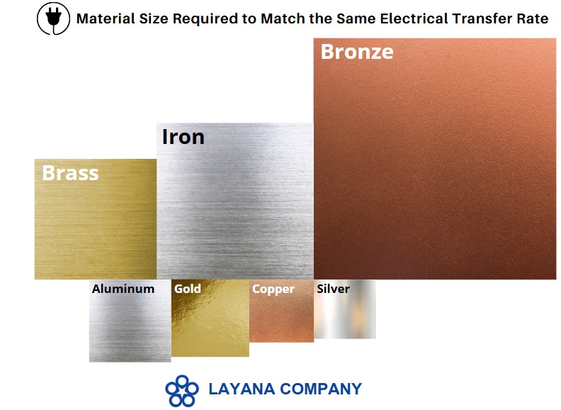
- Copper is the second most electrically conductive metal — about 60% of all copper used worldwide goes into electrical applications.
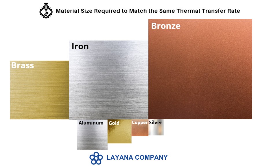
- With a thermal conductivity of ~400 W/m·K, copper is a first-choice material for heat sinks, baseplates and cooling plates.
- For metal stamping, C11000 (ETP copper) is the cost-effective electrical standard; beryllium and chromium coppers add strength for connectors and springs.
- Copper's ductility and malleability make it ideal for intricate progressive-die geometries with minimal material waste.
- Layana delivers copper components under one roof — from DFM and tooling to mass production, finishing and assembly.
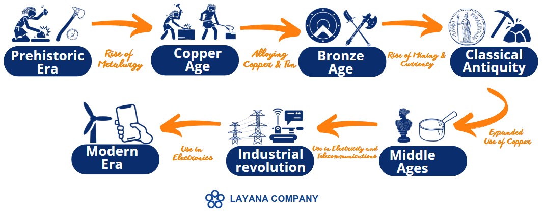
A Brief History of Copper
Copper is one of the most versatile metals in human history — and the first that humankind ever worked. For thousands of years it has driven paradigm shifts in technology: better tools, the electrical grid, the telephone, the smartphone, the electric vehicle, even the journey to the Moon. Few materials have shaped civilization as profoundly.
Native copper and early uses
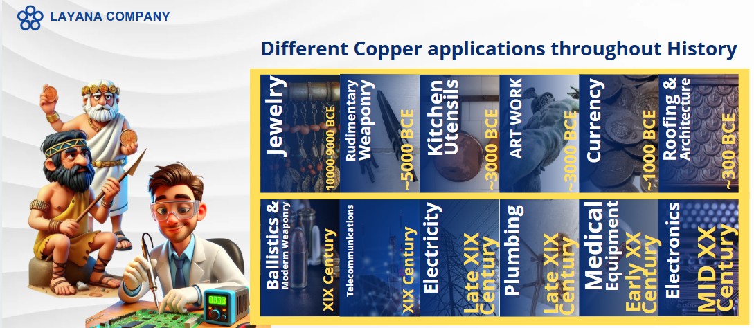
Archaeological evidence suggests copper was first used around 10,000 years ago in the Middle East. In its native, naturally-occurring form it was shaped into rudimentary tools, jewelry, ornaments, hunting gear and cooking utensils — a shift from stone to the first specialized use of metal.
Example: At Çayönü, an ancient settlement in Turkey (c. 9,500–6,500 BC), small copper tools and beads have been discovered.
The rise of metallurgy
The Chalcolithic Period marked the beginning of metallurgy. People began extracting copper from ores to make more complex tools, weapons and ornaments. Early work was done by hammering; the discovery of smelting then enabled purer copper and higher-quality, more intricate parts.
Chemistry: Smelting heats copper ore with a reducing agent such as carbon to produce pure copper. Example: Ötzi the Iceman (c. 3,300 BC) carried a near-pure copper axe, now in the South Tyrol Museum of Archaeology, Italy.
The rise of alloying
Copper was alloyed with tin to create bronze — far stronger and more durable — ushering in the widespread use of bronze tools, weapons and armor. Mesopotamia, ancient Egypt and the Indus Valley flourished in this era.
Composition: Bronze is an alloy of copper and tin, typically 85–90% Cu and 10–15% Sn. Example: A Bronze Age sickle from Ur (c. 2,500 BC) is held in the British Museum, London.
Copper mining and trade
Technical mining expanded. Greeks and Romans relied on copper for coins, plumbing and building materials alongside agricultural tools and weaponry. Trade routes were established across the Mediterranean, Anatolia and the Balkans.
Example: The Roman Empire's extensive use of copper in plumbing and aqueduct systems demonstrates its importance in this period.
Rising demand & better mining
Demand for copper and its alloys continued — for kitchen utensils, weaponry, bells, statues and architecture. Mining and metallurgy techniques improved, particularly across Western Europe.
Example: Copper roofing on landmark European architecture testifies to its enduring use in building during this period.
Electricity & telecommunications
Copper became essential to the rise of electricity and telecommunications. Its conductivity made it the ideal material for electrical wiring and for the telephone and telegraph networks that connected the world. Copper stamping emerged as a crucial process for mass-producing the components these technologies required.
Example: The telegraph, which relied heavily on copper wiring, revolutionized long-distance communication.
Copper in electronics & clean energy
The electrical, construction, electronics and green-energy sectors all rely on copper — from power generation and distribution to internet and satellite networks. Its role now extends to new mobility (electric vehicles) and clean-energy systems such as solar panels and wind turbines.
How Copper Is Used in Manufacturing
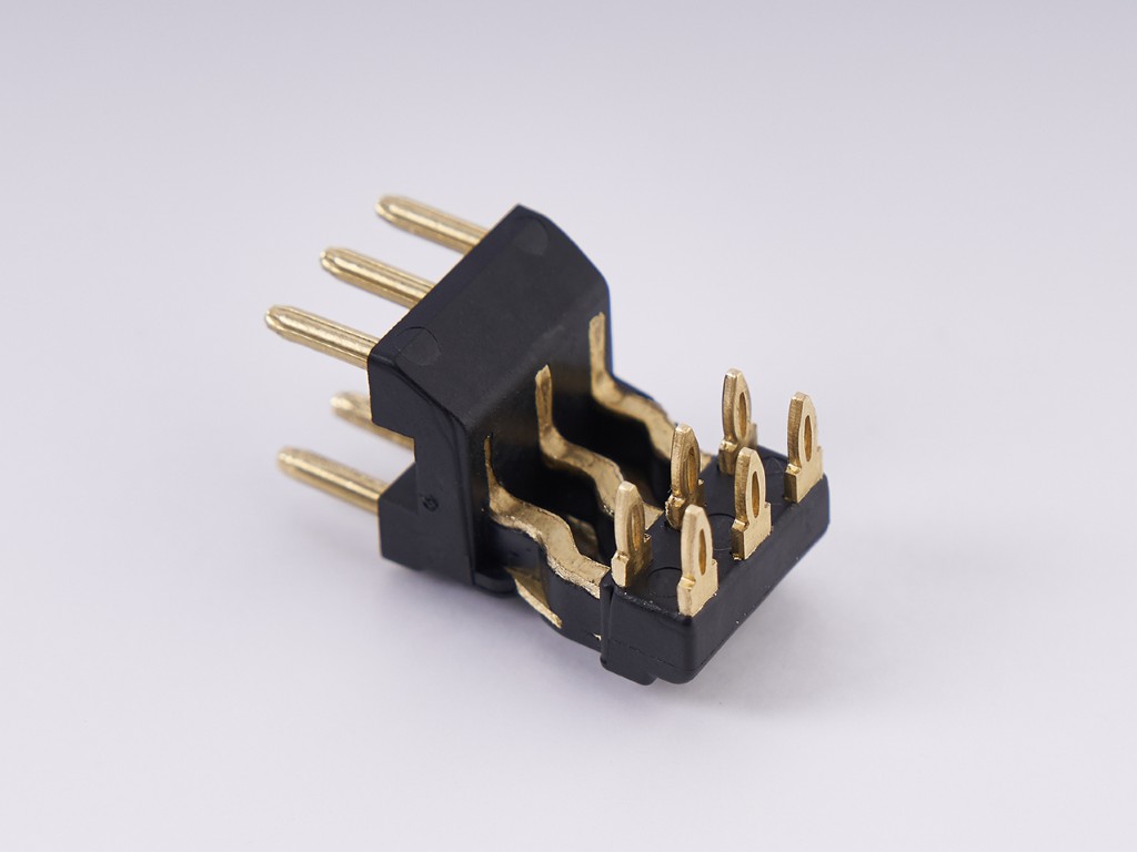
The unique properties of copper make it an ideal material for metal stamping — shaping sheet or coil into precise designs with high accuracy, speed and repeatability at a low defect rate, exactly what mass-production electronics, automotive and telecommunications demand.
Metal stamping forms materials such as copper, aluminum or stainless steel into intricate geometries through a process that produces components with high accuracy and repeatability — essential for reaching mass-production scale without sacrificing quality.
Layana handles every stage of a stamped-copper project — from Design for Manufacturing (DFM) and tooling to mass production and quality assurance — under one roof, run by engineers who have built precise progressive and transfer dies for world-class OEMs.
We also specialize in bi-material processing — combining overmolding and insert molding with metal stamping — to cut assembly steps, reduce cost and improve material efficiency, while our in-house automation team scales projects seamlessly.
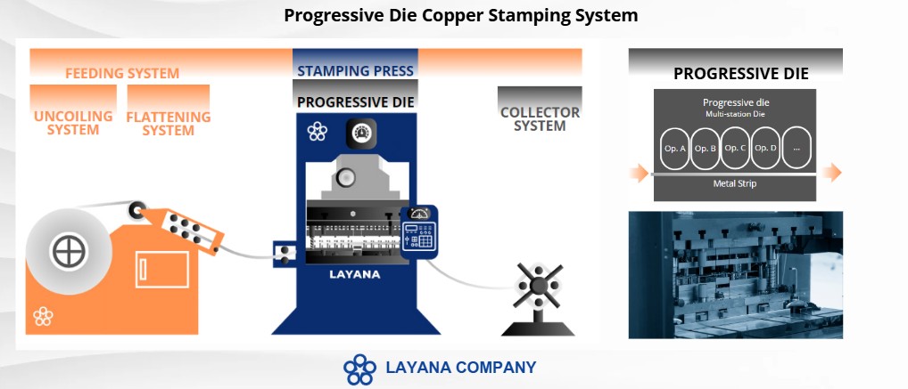
Tooling workshop — In-house progressive and transfer die design and fabrication.
Mass production — High-speed stamping lines with feeding, forming and collection.
Bi-material — Overmolding and insert molding integrated with stamped copper.
Finishing & assembly — Deburring, plating, inspection and component assembly.
Layana's in-house EV power-electronics expertise includes embedded busbars that we progressive-die stamp, then integrate and overmold — delivering weight reduction, fewer assembly steps, and meaningful cost savings.
The Copper Stamping Process
A typical progressive-die copper stamping line moves the strip continuously from feeding, through forming, to collection — in four core stages.
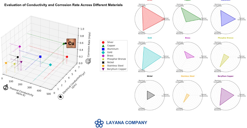
Properties of Copper
Copper's combination of conductivity, ductility and corrosion resistance is what makes it indispensable across electronics, automotive and energy. The headline numbers:
High conductivity — electrical & thermal
Copper is the second most electrically conductive material, owing to an atomic structure that lets electrons flow with minimal resistance — which is why nearly 60% of all copper goes into electrical applications. At roughly 400 W/m·K it also dissipates heat rapidly, making it the go-to choice for heat sinks, baseplates and cooling plates. In power electronics this dual capability lets a single copper component carry current with minimal loss while shedding the heat that high power densities generate.
Electrical Conductivity
Minimal-resistance current flow for wiring, connectors, contacts, circuit boards, semiconductor packaging and power-module baseplates — consistent across a wide temperature range.
Thermal Conductivity
Around 400 W/m·K dissipates heat away from critical components, preventing overheating in electronics, automotive systems, CPU cooling and HVAC.
Corrosion Resistance
A natural protective oxide layer suits marine, outdoor and industrial environments, even if copper is not immune to every corrosive agent.
Ductility
Drawn into thin wire or stamped into intricate shapes without losing integrity — ideal for detailed parts and accurate fine blanking with minimal waste.
Strength
Around 210 MPa annealed — enough for many structural, electrical and plumbing parts. For extreme hardness, engineers turn to bronze, brass or beryllium copper.
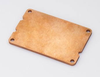
Aesthetic Appeal
A distinctive reddish-orange hue prized in architecture and decor — facades, cladding and interior accents where look and function both matter.
Malleability
Easily shaped, bent and formed without breaking — perfect for stamping, drawing and forming into complex geometries.
Thermal Expansion
A coefficient of about 16.5 x 10^-6 K^-1 — low enough for dimensional stability in electronics and HVAC across temperature swings.
Recyclability
Fully recyclable with no loss of conductivity, strength or malleability — a sustainable choice that conserves resources and energy.
Applications of Copper Metal Stamping
Copper's properties translate directly into four broad families of stamped components across automotive, electronics, energy and industrial markets.
Electrical Components
Connectors, switches, contacts, battery tabs and busbars for efficient power transfer with minimal loss.
Thermal Management
Heat sinks, thermal interfaces and cooling plates for LED lighting, processors and high-power devices.
Decorative & Architectural
Roofing, cladding and ornamental detail combining weather resistance with copper's signature look.
Mechanical Components
Gears, bearings and structural parts where moderate strength meets reliability for industrial and aerospace use.
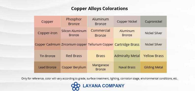
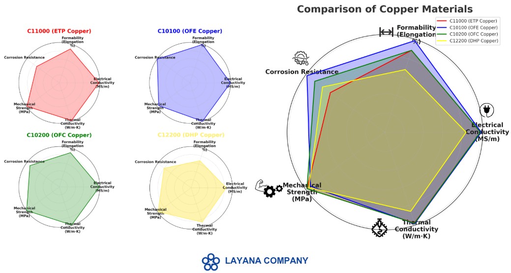
Common Copper Alloys for Stamping
High-purity coppers dominate electrical stamping. The four most common grades trade conductivity against weldability, formability and cost.
| Grade | Conductivity | Key Properties | Typical Applications |
|---|---|---|---|
| C10100Oxygen-Free Electronic (OFE) | ≥101% IACS | ≥99.99% Cu, extremely low oxygen, minimal oxide inclusions, high ductility | Semiconductor components, high-frequency cables, transformer windings, vacuum and electron-tube devices |
| C10200Oxygen-Free Copper | ~101% IACS | ≥99.95% Cu, low oxide content, excellent thermal and electrical performance | Welding rods, precision electronics, vacuum seals, high-performance electrical systems |
| C11000Electrolytic Tough Pitch (ETP) | ~100% IACS | ≥99.90% Cu, outstanding conductivity, best cost-to-performance balance | Power cables, switchgear components, connectors — the most widely used electrical copper |
| C12200Phosphorus-Deoxidized (DHP) | 92–94% IACS | Improved weldability, solderability and corrosion resistance; excellent formability | Plumbing, heat exchangers, applications needing strong thermal performance |
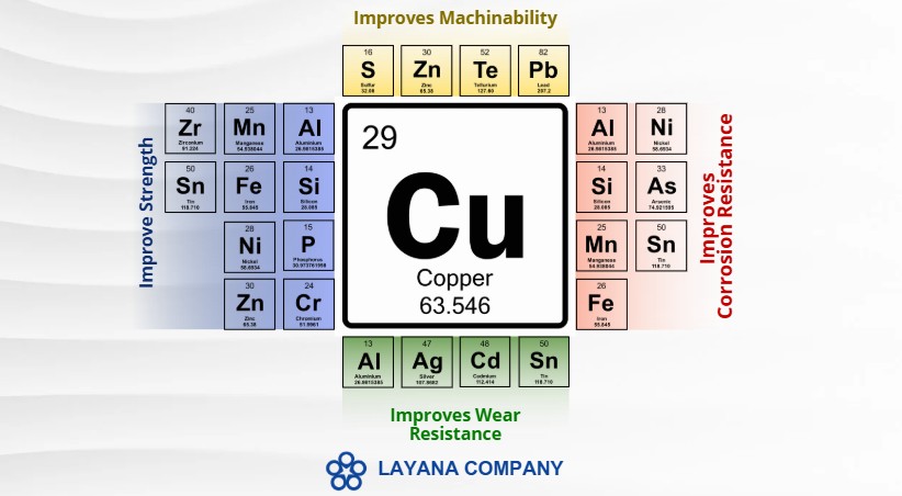
Other Common Copper Alloys
Beyond the high-purity grades, alloying elements tune copper for strength, machinability, corrosion resistance or wear resistance. Expand each family for detail.
Surface Treatments for Stamped Copper
Surface treatments significantly enhance the corrosion resistance, wear resistance, conductivity and appearance of stamped copper parts.
Electroplating
Nickel, tin, silver or gold layers improve conductivity, durability and solderability.
Anodizing
Creates a protective oxide layer for added durability and corrosion resistance.
Passivation
A chemical process that forms a corrosion-resistant film on the surface.
Polishing & Buffing
Produces a smooth, decorative finish and enhances the part's appearance.
Coatings & Paints
Specialized coatings add protection or provide electrical insulation where required.
The Result
Together these processes ensure optimal performance and longevity of copper components across industries.